- Call Us Today!
- +86 519-88123456
- info@ptfe-pcb-laminate.com

2023 10th World Radar Detection and Defence Expo
05/07/2023
Understanding the Benefits of PTFE Prepreg
12/04/2024The electronics industry continually evolves, demanding materials that can withstand high frequencies, extreme temperatures, and provide reliable performance. PTFE (polytetrafluoroethylene) PCB laminate has emerged as a pivotal material in meeting these challenging requirements. This article delves into the advantages of PTFE PCB laminate, exploring its properties, applications, and the manufacturing intricacies that make it a favored choice in high-frequency electronic applications.
Understanding PTFE PCB Laminate
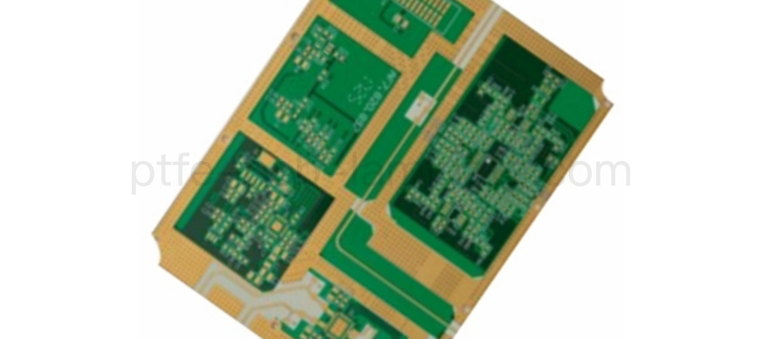
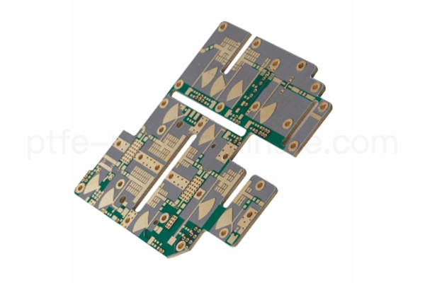
Polytetrafluoroethylene (PTFE) is a synthetic fluoropolymer renowned for its exceptional properties. As a PCB laminate, PTFE is used extensively in radio frequency (RF) and microwave applications due to its low dielectric constant and loss tangent. These properties are crucial for reducing signal distortion and maintaining signal integrity at high frequencies, making PTFE PCB laminates indispensable in modern electronics.
Key Properties of PTFE
- Dielectric Stability: PTFE exhibits a low dielectric constant (approximately 2.1), which remains stable across a wide frequency range. This property is essential for maintaining consistent electrical performance in RF and microwave circuits.
- Low Loss Tangent: The low dissipation factor of PTFE minimizes signal loss, ensuring efficient transmission of high-frequency signals with minimal attenuation.
- Thermal Resistance: PTFE can withstand high temperatures, making it suitable for applications that experience thermal cycling or require high thermal stability.
- Chemical Inertness: The inert nature of PTFE makes it resistant to solvents, acids, and bases, thereby enhancing the longevity and reliability of the electronic components.
- Flexibility and Mechanical Stability: PTFE’s flexibility facilitates its use in a variety of applications, while its mechanical stability ensures durability under stress.
Manufacturing Process of PTFE PCB Laminate
The manufacturing process of PTFE PCB laminate is a sophisticated endeavor, requiring precision and expertise to ensure optimal material performance. Here’s a step-by-step overview:
1. Creation of PTFE Coated Fiberglass Fabric
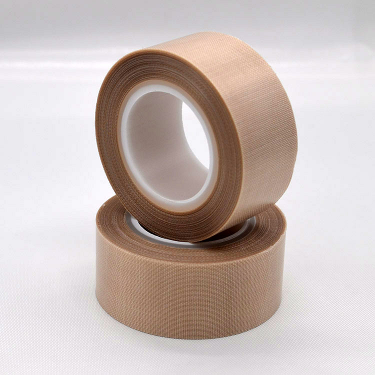
The process begins with the impregnation of fiberglass fabric with PTFE resin. This step is critical as it defines the foundational properties of the laminate. The fiberglass provides structural support, while the PTFE resin imparts its unique electrical properties.
2. Drying and Sintering
Post impregnation, the fabric undergoes a drying process to remove solvents. Following this, sintering is performed, where the material is exposed to high temperatures. This step is crucial for achieving the desired mechanical and chemical properties of PTFE.
3. Pressing of PTFE Laminate
The PTFE-coated fiberglass is then pressed under controlled temperature and pressure conditions to form the laminate. This pressing process ensures uniform thickness and density, which are vital for consistent electrical performance.
4. Quality Control and Testing
Following the pressing, rigorous quality control measures are implemented to ensure the laminate meets specified criteria. Testing for dielectric constant, loss tangent, and thermal stability are conducted to verify the material’s suitability for electronic applications.
Applications of PTFE PCB Laminate
High-Frequency Electronics
PTFE PCB laminates are primarily used in high-frequency electronics, including RF and microwave applications. Their low dielectric constant and loss tangent make them ideal for antennas, power amplifiers, and other components where signal integrity is paramount.
Aerospace and Defense
In aerospace and defense, PTFE laminates are utilized in radar systems, communication devices, and electronic warfare equipment. The material’s thermal resistance and chemical inertness ensure reliability in harsh environments.
Telecommunications
The telecommunications industry relies on PTFE laminates for base station antennas and satellite communication systems. The material’s ability to maintain signal clarity over long distances is a significant advantage.
Medical Devices
PTFE laminates are also employed in medical devices that require high precision and reliability. Their biocompatibility and stability make them suitable for implantable devices and diagnostic equipment.
Advantages Over Other PCB Materials
Superior Electrical Performance
Compared to traditional FR-4 laminates, PTFE offers superior electrical performance, particularly in high-frequency applications. Its low dielectric constant and loss tangent are unmatched, providing an edge in applications where signal integrity is critical.
Enhanced Thermal Management
PTFE’s excellent thermal properties allow it to perform effectively in high-temperature environments, reducing the risk of thermal-induced failures.
Long-Term Reliability
The chemical inertness and mechanical stability of PTFE result in long-term reliability, reducing maintenance requirements and extending the lifespan of electronic components.
Conclusion
PTFE PCB laminates represent a pinnacle of innovation in the electronics industry, offering unmatched performance in high-frequency, high-reliability applications. Understanding the properties, manufacturing process, and applications of PTFE laminates enables electronics manufacturing managers to make informed decisions, ultimately improving production efficiency and product quality. Embracing PTFE technology is not merely about keeping up with industry standards; it’s about setting new ones.
By leveraging the unique advantages of PTFE PCB laminates, industries can drive advancements in technology, ensuring that electronic systems are more efficient, reliable, and robust than ever before. The future of electronics is here, and it’s PTFE-driven.


